lab grown diamonds
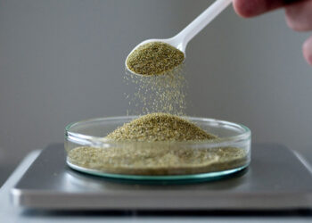
Nanometer Modified Diamond Powder
lab grown diamonds
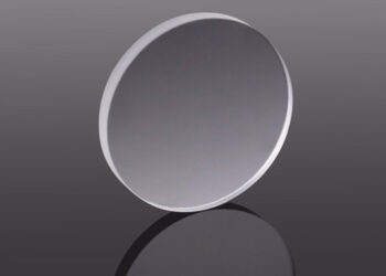
CVD SC Diamond Optical Window
lab grown diamonds
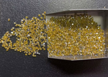
HPHT Monocrystalline Diamonds


lab grown diamonds
lab grown diamonds
lab grown diamonds