Project Details
- Product Name:
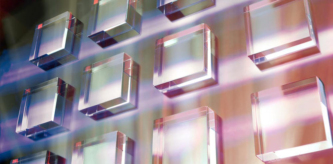
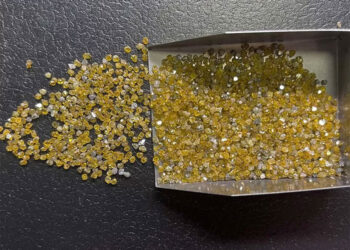
Single Crystal CVD Plate
- Type::
Optical Grade
- Crystal Orientation:
100 110 111
- Usage:
Making Tools, As Seed
- Technology:
CVD
CVD Single Crystal Diamonds are produced by CVD method. The mobility and lifetime of single crystal CVD diamond layers are more than 320 x 10″6 cm2/V and 1.5 x 10″6 cm2/V, respectively. The stock material for CVD Single Crystal Diamonds is selected based on microscopic examinations and birefringence imaging. The stock material was processed by laser lapping and sawing process to minimize the subsurface defects. Then, the defects were identified and quantified by plasma etching.
Characteristics of CVD Single Crystal Diamonds
CVD single crystal diamonds can be designed with a variety of different properties depending on their application. The CVD method has enabled diamonds to be fabricated with mobility and lifetime exceeding 5 x 1014 cm2/V. The CVD technique also allows for tailoring different grades of diamonds for different purposes. For example, large area polycrystalline diamond plates have been developed for use in detectors and RF windows. These applications will require different optimized grades of diamond.
- The CVD process produces diamonds with various spectroscopic properties. The first CVD experiment was conducted in 1952, and the process was later adapted for industrial production. CVD diamond synthesis can be done in a range of hydrothermal conditions, including metastable conditions, and has been successfully applied to produce diamonds with large areas.
Gemological properties of CVD Single Crystal Diamonds :
Single-crystal diamonds are synthetically produced through the use of a process called CVD. This process uses plasma and high-pressure to produce diamond crystals. After the initial rotational phase, these crystals grow vertically with no lateral growth. The process also produces diamonds of high purity.
- The top surface of single-crystal diamonds must be uniform and controlled. These diamonds must be packed densely in a carrier substrate to shield the sides that are not growth faces. They must also present a single growth face to plasma. The side walls of the carrier substrate must be in close proximity to the single crystal diamond substrate. This arrangement allows for a high degree of control over the top surface of the diamond.
- For the CVD method to be successful, the gas must contain at least 90% hydrogen. This is to ensure that the gas is sufficiently activated. The gas is then forced to split the hydrogen molecules, converting the double bonds in graphite into diamond bonds. However, this method is slow and requires large quantities of atomic hydrogen. Hence, it is suited for small-scale production, where the area to be processed is small.
CVD Lab Grown Diamonds CVD Single Crystal Diamonds:
Single-crystal diamonds are synthetically produced through the use of a process called CVD. This process uses plasma and high-pressure to produce diamond crystals. After the initial rotational phase, these crystals grow vertically with no lateral growth. The process also produces diamonds of high purity.
CVD single crystal diamonds have a low cost and a wide range of applications. They are used in lasers, as optical components, as windows, and as electrodes for ozone generation, electrochemical sensing, and direct oxidation of organic materials. They are also used in high-power electronics, as erosion-resistant coatings for nuclear fusion reactors, and in quantum optics. Moreover, these diamonds are available in high purity and low defect grades.
Single crystal diamonds are the ultimate material for high temperature, high voltage, and high frequency applications. Their outstanding resistance to radiation makes them an excellent material for these purposes. In addition, they can host a range of colorcenters, including color centers involving impurities. This makes them the perfect diamond for laser and microwave applications.
CVD diamonds are made using a chemical process based on chemical vapour deposition, which was first performed in 1952. The technique was later industrialized and has since been used to make polycrystalline diamonds. The technology has since been used to create synthetic diamonds in a metastable regime.
CVD Single Crystal Diamond is a material that can be fabricated using CVD process. Its unique properties make it an excellent choice for high power transmission windows. These windows also benefit from a low coefficient of thermal expansion. However, they are susceptible to thermal stress, which can reduce their lifetimes and reliability. In such cases, it may be desirable to use a pre-cracked compound semiconductor or diamond sandwich to balance the thermal stresses. Moreover, CVD diamonds can be fabricated on a copper block to reduce device temperature rise.
Diamond devices can also be used to manufacture power devices. The power output can be high, and the operation temperature can be high. To make such a device, it is important to develop the process as rapidly as possible. In the case of power devices, the target dislocation density should be less than 0.1 cm-2 and the resistivity should be less than 0.005 O cm. In addition, the initial diamond wafer must be 4 inches in size.
As the physical properties of single crystal diamond are highly unique, it is an ideal material for quantum devices and power electronics. The color centers hosted in the diamond lattice are important in quantum devices. At present, two synthesis methods are being explored to grow high-quality diamonds. The first method involves high temperature and pressure synthesis. The second method is chemical vapor deposition. In this method, a diamond crystal nucleate is formed on a foreign substrate under controlled conditions.
In addition to being low-temperature, CVD single crystal diamonds can be produced with low-birefringence. This means that it can be used to improve the performance of doped dielectric lasers and semiconductor disk lasers.
Single-crystal diamonds are synthetically produced through the use of a process called CVD. This process uses plasma and high-pressure to produce diamond crystals. After the initial rotational phase, these crystals grow vertically with no lateral growth. The process also produces diamonds of high purity.
The top surface of single-crystal diamonds must be uniform and controlled. These diamonds must be packed densely in a carrier substrate to shield the sides that are not growth faces. They must also present a single growth face to plasma. The side walls of the carrier substrate must be in close proximity to the single crystal diamond substrate. This arrangement allows for a high degree of control over the top surface of the diamond.
For the CVD method to be successful, the gas must contain at least 90% hydrogen. This is to ensure that the gas is sufficiently activated. The gas is then forced to split the hydrogen molecules, converting the double bonds in graphite into diamond bonds. However, this method is slow and requires large quantities of atomic hydrogen. Hence, it is suited for small-scale production, where the area to be processed is small.
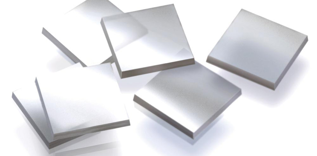
Single-crystal CVD diamonds are generally 8-20 mm thick. They can be used in optical devices. Single-crystal CVD diamonds are also useful for thermal management in laser systems. They can be used as a substrate for semiconductor disk lasers or doped dielectric lasers.
Related Projects
lab grown diamonds
Nanometer Modified Diamond Powder
lab grown diamonds
CVD SC Diamond Optical Window
lab grown diamonds